Silicon photonics builds optical functions into semiconductor chips so selected data connections can carry information as light. Electronic circuits still prepare the data, drive optical components and recover the received signal. The useful change is where and how communication happens—not replacing a GPU’s calculations with beams of light. [1] [4] [5]
This guide follows a signal from the laser through a modulator, waveguide and fibre to the receiver. It explains why silicon needs help to provide the light source, how multiple wavelengths share a connection, and why a headline such as “4 Tb/s bidirectional” needs careful reading. It also separates optical processor I/O from co-packaged switch optics, two related ideas that solve different connection problems. [2] [3]
Show less
On this page 13 sections
- Key Takeaways
- What silicon photonics puts on a chip
- How a silicon-photonic data link works
- Why light frequency is not the same as data bandwidth
- Reading “4 Tb/s bidirectional” correctly
- CPO and optical processor I/O are related, not identical
- What optical connections can—and cannot—do for AI
- Why copper still has a role
- The optical chip still needs a reliable package
- Important Points / Key Information
- Examples / Supporting Information
- Common questions about silicon photonics
- Conclusion
Part of our computer hardware technology guide library
Key Takeaways
- Silicon photonics combines optical functions with electronic drivers, receivers and control; it does not replace GPU arithmetic.
- A silicon-photonics system can integrate lasers made from other semiconductor materials.
- WDM shares an optical path between wavelength channels, but its capacity still depends on the complete link design.
- Intel’s documented approximately 4 Tb/s bidirectional example is about 2 Tb/s in each direction; switch-wide aggregates describe a different boundary.
What silicon photonics puts on a chip
A photonic integrated circuit, or PIC, brings optical components together on a chip. A waveguide provides a path for light. A modulator encodes data onto that light. Filters and couplers manage the route and wavelength channels, while a photodetector converts received light into an electrical signal. The available components depend on the manufacturing platform and design. [1] [5]
Silicon photonics uses semiconductor fabrication techniques, including lithography and etching, to build these structures. But a photonics process is not simply an ordinary processor process with a different circuit layout. Imec describes platforms with dedicated optical building blocks and ways to integrate other materials; its earlier technical explanation describes a modified CMOS process with germanium detectors and optical coupling structures. [1] [5]
Why the material is not always just silicon
Silicon is useful for guiding light in suitable infrared wavelength ranges. That is not a claim that silicon is transparent to every visible colour. The material and wavelength must match the intended optical function.
Pure silicon is not an efficient conventional laser material. Practical silicon-photonics systems can receive light from an external laser or integrate a laser made using other semiconductor materials. Imec describes adding III–V lasers to a silicon-photonics platform, while Intel describes heterogeneously integrated indium-phosphide laser technology. An “on-chip laser” in such a system does not mean pure silicon suddenly became an efficient light emitter. [1] [4]
Germanium is another useful addition. Imec’s technical description uses germanium photodetectors with silicon waveguides. Different parts of the system can therefore use different materials, chosen for light generation, guidance, modulation or detection. [5]
How a silicon-photonic data link works
The link keeps moving between electronic and optical functions. A simple description is enough to show why a photonic chip still needs drivers, receivers, control and careful packaging. Imec describes a photonic circuit assembled with electronic driver and receiver circuits; Intel’s optical-compute interconnect similarly combines a PIC with an electronic integrated circuit. [2] [5]
- Prepare the electrical data. The electronic transmitter presents a signal in the format required by the link and drives the optical transmitter circuitry.
- Provide and modulate laser light. The light source supplies the optical carrier. A modulator changes an optical property in response to the electrical data; the exact modulation scheme is design-specific.
- Guide the optical signal. Light travels through an on-chip waveguide and couples into fibre or another supported optical path. A wavelength multiplexer can combine channels when the design uses multiple wavelengths.
- Detect and recover the data. At the other end, the optical signal reaches a photodetector. Receiver electronics amplify and recover the information from its small electrical output.
Why the modulator matters as much as the laser
The laser provides light, but the data rate is not set by simply having a powerful or high-frequency laser. The modulator must encode information at the required rate, and the electronic driver must deliver a suitable signal. The detector and receiver then need enough performance to recover it reliably. [5]
Different designs use different modulation mechanisms. A Mach–Zehnder interferometer uses the relationship between optical paths to affect the output; a ring-resonator design uses an optical resonance; an electro-absorption device changes how much light is absorbed. These are alternatives with their own requirements, not interchangeable names for one component.
Temperature can shift the behaviour of wavelength-selective optical structures. Control or tuning may therefore be needed to keep the intended channels working. Imec specifically identifies temperature-sensitive wavelength filters and insertion loss as trade-offs in wavelength-multiplexed links. [5]
Why light frequency is not the same as data bandwidth
An optical carrier’s oscillation frequency is not the number of data bits transmitted each second. A useful link rate depends on how information is encoded and how much of that modulation the whole transmitter-to-receiver system can support.
Modulator speed, receiver bandwidth, signal quality, optical loss and the selected encoding all matter. Error correction and other protocol overhead can also make usable application throughput lower than the advertised raw line rate. Counting optical oscillations does not establish either figure.
This is why real demonstrations describe channels, signalling rates, wavelengths and error measurements. Intel’s 2024 optical I/O demonstration, for example, reported channels running at 32 Gb/s and included optical-spectrum and bit-error-rate measurements. It did not treat the laser’s carrier frequency as the link’s data rate. [2]
How several wavelengths share an optical connection
Wavelength-division multiplexing, or WDM, places multiple optical channels at different wavelengths onto a shared optical path. A multiplexer combines them at the transmitter; a corresponding receiver arrangement separates and detects the intended channels. It is one way to increase aggregate capacity without adding a separate fibre for every channel. [2] [5]
The channels are not automatically immune to interaction. Wavelength spacing, filtering, available optical power and loss must be suitable for the design. Multiplexing also introduces components and control requirements; it does not provide unlimited capacity at no cost. [5]
In Intel’s documented 2024 example, eight fibre pairs each carried eight wavelength channels. With 32 Gb/s per channel, eight channels account for 256 Gb/s in one direction on the relevant fibre. Across 64 channels, the one-direction total becomes 2,048 Gb/s. Those totals describe that example, not every silicon-photonics product. [2]
Reading “4 Tb/s bidirectional” correctly
Intel’s June 2024 announcement described an optical-compute interconnect chiplet designed for 64 channels at 32 Gb/s in each direction. It called the first implementation approximately 4 Tb/s bidirectional. Read the channel arithmetic before assuming that 4 Tb/s is available in each direction. [2]
The calculation is 64 × 32 Gb/s = 2,048 Gb/s, or 2.048 Tb/s, in one direction. Summing both directions gives 4.096 Tb/s, which is approximately 4 Tb/s bidirectional. This is an aggregate signalling-capacity calculation from the stated channel figures; it is not a measured application-throughput result.
At OFC 2024, Intel showed the chiplet co-packaged with a CPU and running live data. The announcement described the chiplet as a prototype and gave a design reach of up to 100 metres, while noting that practical uses could be limited to shorter distances by propagation latency. These are dated demonstration details, not proof that every CPU or GPU now ships with optical I/O. [2]
Intel’s current photonics overview still describes first-generation OCI support as 4 Tb/s bidirectionally and discusses evaluation platforms. It separately lists 800 Gb/s and 1.6 Tb/s transceiver components. A component listing and an optical-compute demonstration establish different things; neither should be rewritten as universal availability in production AI servers. [4]
CPO and optical processor I/O are related, not identical
Co-packaged optics, or CPO, describes putting optical engines close to a main chip within a shared package or tightly integrated package assembly. In switch CPO, the optical engines sit near the switching ASIC, shortening the electrical path that would otherwise cross the board to faceplate modules. NVIDIA’s technical description presents that switch-side architecture. [3]
Optical processor I/O targets connections associated with the compute package. Intel’s OCI example places an optical I/O subsystem with a CPU; the concept can also be designed around other processors. It concerns how data enters and leaves compute devices rather than how a switch’s optical ports are packaged. [2] [4]
A PIC is the optical circuit. CPO is an integration arrangement. Optical I/O describes a communication function. A design can combine them, but the terms are not synonyms—and none establishes that the main processor performs its arithmetic optically.
A switch’s total capacity is not one optical link
NVIDIA’s August 2025 technical article described a Spectrum-X Photonics SN6810 platform with 128 ports at 800 Gb/s, giving 102.4 Tb/s in aggregate. It also described a larger 512-port platform with 409.6 Tb/s. These are platform-wide capacity figures, not the rate of one fibre and not the memory bandwidth of one GPU. [3]
The document also gave planned 2026 availability dates. A date in a 2025 roadmap is not evidence that the planned shipment has happened everywhere. This guide uses the documented architecture and rate boundaries; it does not claim independently verified rollout volumes, customer installations or Indian availability.
What optical connections can—and cannot—do for AI
Some distributed AI workloads exchange model data, activations or synchronisation information across several processors. A communication-limited workload may spend time waiting on those exchanges even when individual accelerators are fast. Not every AI model needs thousands of GPUs, and not every inference task has the same network demand. [2] [3]
Optical connections can address selected reach, bandwidth-density and electrical-channel constraints. They cannot by themselves repair an inefficient communication pattern, a congested topology or insufficient local memory bandwidth. Data still needs to be scheduled, routed and consumed by the application.
For that reason, a faster external connection should not be called a replacement for high-bandwidth memory. Links between packages and the local memory interface serve different parts of the data path. A useful system needs the right balance rather than the largest isolated bandwidth number.
Why copper still has a role
Electrical links remain useful where their reach, power, cost and packaging fit the requirement. There is no universal distance at which every copper link fails. The signalling rate, channel materials, connectors and compensation techniques determine what a specific connection can support.
Optics introduces its own transmitter, light source, coupling, receiver and control costs. Shortening a difficult electrical path can help, but moving conversion closer to a chip does not make those costs vanish. Compare complete links at the same required performance and reach—not an optical component against an entire electrical system. [2] [3] [4]
Energy per bit needs a clear boundary
Energy per bit expresses how much energy a defined part of the system uses relative to the bits it moves. It can be useful, but the comparison must identify whether lasers, drivers, receivers and tuning are included, as well as the traffic rate and operating conditions.
For an illustrative calculation only, suppose a complete defined link consumed 6 picojoules per transferred bit while carrying 1 terabit per second. Multiplying 6 × 10⁻¹² joules by 10¹² bits per second gives 6 watts. This is a hypothetical constant-energy-per-bit example, not a measurement of an Intel or NVIDIA product.
Real hardware can consume power while idle, so halving traffic does not necessarily halve total power. Cooling and other system overhead also lie outside some link-level measurements. A claim of better energy per bit is therefore not automatically a claim of lower total facility energy. [2] [3]
The optical chip still needs a reliable package
Light must couple into and out of the PIC with acceptable loss. Fibre attachment, alignment and protection therefore remain part of the working system. Electronic connections, thermal management and test access must fit alongside the optical path. Foundry-supported devices alone do not complete that assembly. [1] [4]
Laser placement affects both integration and service. An external source and a heterogeneously integrated source create different physical and maintenance choices. Intel emphasises integrated laser manufacturing and testing, while imec describes several ways to add active optical materials. Neither approach means all implementations share one service model. [1] [4]
For Indian readers following semiconductor development, the useful questions are which process supports the design, how the optical package is assembled and tested, and what the complete link has demonstrated. This is an engineering learning point, not a claim of domestic manufacturing, local deployment or a guaranteed timetable.
Important Points / Key Information
Silicon photonics becomes easier to understand once the component, connection and system boundaries are kept separate.
- A PIC manages optical functions; electronic drivers and receivers remain essential. [4] [5]
- A laser integrated with silicon can use another semiconductor material. On-chip does not mean pure-silicon light generation. [1] [4]
- Optical carrier frequency is not the line rate or application throughput.
- WDM combines wavelength channels but still needs suitable spacing, loss, filtering and control. [2] [5]
- A summed bidirectional figure is different from a per-direction rate; a switch-wide aggregate is different from one port. [2] [3]
- Dated demonstrations and planned availability must not be treated as universal current deployment.
Examples / Supporting Information
For a component-level example, Intel’s current overview lists transmit and receive PICs alongside driver, receiver-amplifier and controller components for transceiver designs. It makes visible the electronics that still accompany the photonic circuit. [4]
For a compute-side example, the 2024 OCI demonstration combined a photonic and electronic die stack with a CPU and tested live communication between platforms. For a switch-side example, NVIDIA’s technical description moves optical conversion near the switch ASIC. Both bring optics closer to electronics, but they operate at different points in a computing system. [2] [3]
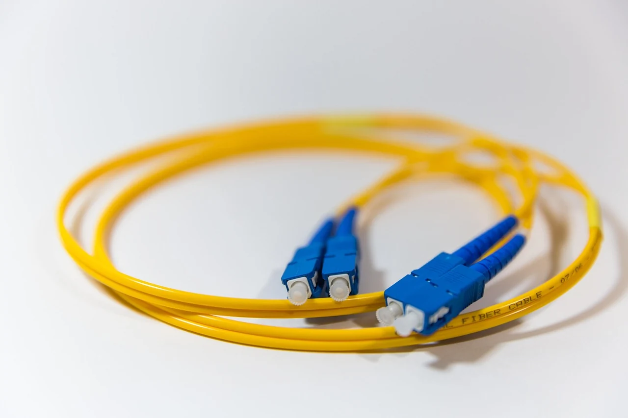
These are documented examples, not TechDuoPulse hardware tests. The real cable photograph illustrates an ordinary external fibre connection; it does not show the microscopic waveguides or establish the optical performance of either design.
Common questions about silicon photonics
Does silicon photonics always need an external laser?
No. Some systems use an external light source, while others integrate lasers using additional semiconductor materials. Intel’s documented approach includes on-chip lasers through heterogeneous integration. The distinction is between where the laser sits and what material produces the light. [1] [4]
Does silicon photonics replace the GPU?
Not in the communication architectures described here. It changes selected data connections around processors or network equipment. The processor still performs its electronic computation; optical I/O is not the same claim as an optical-computing processor. [2] [3]
Does optical I/O remove every memory bottleneck?
No. External connectivity is only one part of data movement. Local memory capacity, memory bandwidth, software and communication patterns can still limit a workload. A fast optical link should not be treated as a substitute for a balanced compute-and-memory design.
Does “4 Tb/s bidirectional” mean 4 Tb/s each way?
Not in Intel’s stated 2024 example. Its 64 channels at 32 Gb/s amount to 2.048 Tb/s in each direction, or 4.096 Tb/s summed across both. Always check how a document defines its aggregate. [2]
Conclusion
Silicon photonics changes selected communication paths by integrating optical functions with semiconductor manufacturing and electronic control. The practical link is a chain: light source, modulation, optical guidance, detection and electronic recovery. Its performance depends on that chain, not merely on the presence of light.
The clearest way to read a photonics announcement is to identify the component and its role, then check the direction, channel count and capacity boundary of every rate. Keep demonstrations separate from deployment claims and switch optics separate from compute I/O. That approach explains where the technology helps AI infrastructure without implying that it removes every data-movement or energy constraint. [2] [3] [4]
How we checked thisSources (5)
We keep source links private so your reading stays on techduopulse. Each note names the publisher and document we checked.
imec — Silicon photonics foundry services
Primary source · Photonic components, process platforms and III–V laser integrationIntel — Intel Demonstrates First Fully Integrated Optical I/O Chiplet
Primary source · Historical OCI prototype, CPU co-packaging, channels, rates and reachNVIDIA — Scaling AI Factories with Co-Packaged Optics for Better Power Efficiency
Primary source · Switch CPO architecture and platform-wide capacity boundaries; roadmap dates not reported as completed rolloutIntel — Intel Silicon Photonics — Integrated Photonics Solutions
Primary source · Current component listings, heterogeneous lasers, electronic subsystems and OCI descriptionimec — New silicon photonics technology delivers faster data traffic in data centers
Primary source · Evergreen component explanation: modified fabrication flow, germanium detection, drivers, receivers and wavelength-control trade-offs; old roadmap not reusedInitial source-backed manual publication. Existing reviewed article facts and original licensed real photograph preserved. Full article remains server-rendered, keyboard accessible and printable behind a two-paragraph reading disclosure.