Computing systems increasingly spend engineering effort moving data among processors, memory, accelerators, and network equipment. Electrical interconnects remain indispensable, but long or very high-rate electrical channels can face signal-integrity, power, and routing constraints. Silicon photonics uses semiconductor-fabricated optical components to encode, guide, modulate, and detect light for communication. The key word is selective: optical links can alter a data path’s trade-offs, yet they still need electrical drivers, receivers, packaging, control, and a connection to the workload that benefits from them.
This article is part of the computer hardware technology guide library.
The bottleneck is movement, not only computation
A data-movement bottleneck occurs when useful computation waits on information to arrive, or when the energy and infrastructure required to move that information become a limiting resource. It can appear on a board, between racks, across a data centre, or inside a tightly integrated package. The bottleneck is workload-dependent. A calculation with high reuse may be compute-limited, while one that repeatedly streams or exchanges large data sets may be constrained by communication bandwidth, latency, or contention.
Electrical links are not a failed technology; they are the foundation of most digital systems. Their properties depend on channel length, frequency content, connectors, materials, equalisation, and topology. Silicon photonics is relevant where using light for part of a connection could provide a more suitable bandwidth, reach, density, or energy trade-off. It should be evaluated as a link architecture, including its electro-optic conversion overhead, rather than as a claim that photons make every communication path universally faster or cheaper.
What a photonic integrated circuit does
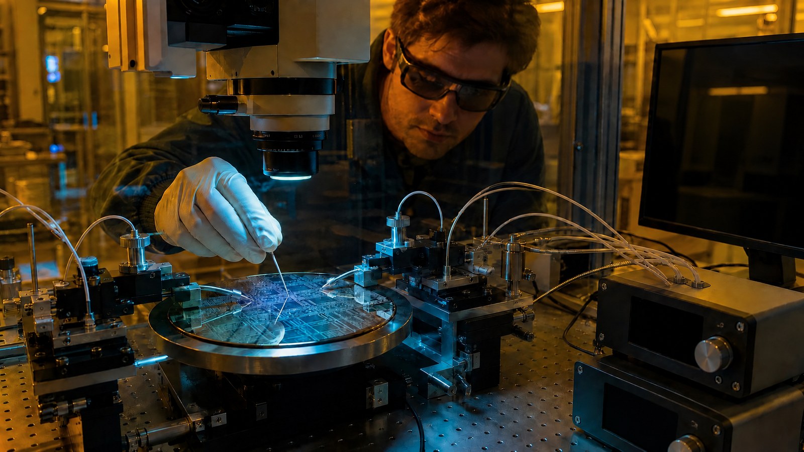
A photonic integrated circuit, often called a PIC, places optical functions on a chip or closely integrated substrate. Depending on the design, those functions can include waveguides that direct light, modulators that encode data, filters that separate wavelengths, and photodetectors that turn light back into electrical signals. Silicon is attractive because semiconductor manufacturing techniques can support dense optical structures and integration with electronic design and packaging workflows, though a complete optical system may use more than one material or component type.
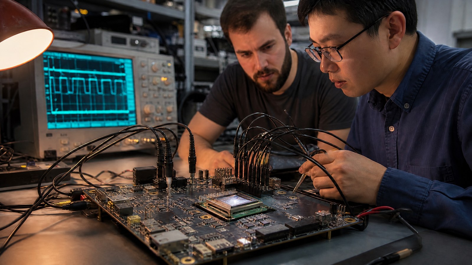
The optical path is only one part of the communication system. Electronics must generate and condition data, drive modulators, recover received signals, provide clocks and control, and manage faults. Light sources may be integrated or separately coupled. Fibre or other optical coupling must be aligned and retained. NIST’s electronics-and-photonics programme explicitly focuses on advanced packaging techniques that combine photonics and electronics for high-speed data communication, a reminder that integration—not a bare PIC alone—determines the practical link.
Wavelengths can share a path
Wavelength-division multiplexing, or WDM, carries multiple optical channels at different wavelengths through a shared optical path. It can increase the information carried by a fibre or waveguide without simply duplicating the entire route for every channel. That possibility is one reason integrated photonics is studied for high-capacity data links. It also adds control and design requirements: wavelengths must be generated, selected, stabilised, and received with sufficient separation and signal quality for the intended system.
NIST describes research on microresonator frequency combs as multi-wavelength sources for data communication and reports work integrating photonics and electronics for a high-speed optical link. Such research establishes technical possibilities under described conditions; it does not make every optical system a frequency-comb system or establish an automatic deployment outcome. In an engineering decision, the question is whether the source, modulation, receiver, packaging, control, and temperature behaviour collectively meet the link budget and operational requirements.
Packaging decides whether the optical link survives reality
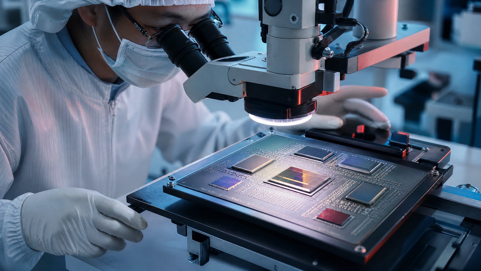
Photonic packaging connects a delicate optical circuit to fibres, electrical connections, thermal paths, and a mechanical enclosure. Alignment matters because light must couple between components with limited loss. Packaging must also tolerate handling, vibration, temperature change, and manufacturing variation. These needs can be more exacting than simply mounting an electronic die. A prototype that demonstrates an optical function on a bench has not yet answered how the link will be assembled repeatedly, protected, tested, and maintained in a system.
AIM Photonics describes an end-to-end development infrastructure that includes design, simulation, fabrication, packaging, validation, and a path to volume manufacturing. That sequence captures an enduring truth: the handoff between photonic design and assembly is part of the technical work. Designers need to consider fibre attachment, laser strategy, electrical input/output, thermal control, test access, and connectorisation early. Leaving those decisions to the final enclosure can force changes that undermine the optical performance the chip demonstrated in isolation.
Energy is a link-level accounting problem
Optical communication can be attractive for its potential energy characteristics at high bandwidth and over distances where electrical signalling becomes demanding. But energy claims need a stated boundary. A link consumes energy in drivers, modulators, light sources, control circuits, receivers, and sometimes thermal stabilisation. The useful comparison includes the complete transmit-to-receive path at the required error performance, reach, and traffic pattern. Quoting only an optical component’s consumption risks leaving out the equipment that makes it communicate.
NIST identifies energy consumption as a key performance driver for scaling data-centre interconnects and distributed or high-performance computing architectures. That is a reason to investigate integrated optical approaches, not a result that can be assumed for every topology. System designers should account for idle power, utilisation, conversion overhead, management, and cooling alongside active data transmission. The result may favour photonics for a particular high-throughput path, while another path remains better served by electrical wiring because its distance, bandwidth, or cost requirements differ.
How to judge a silicon-photonics proposal
First, define the data path and its constraint. Is the pain point channel loss, bandwidth density, reach, energy, port count, or a combination? Next, identify each conversion and interface: electronic transmitter, optical source, modulator, coupling, fibre or waveguide, detector, receiver, and control plane. Then ask how the package is built and tested. This turns a broad photonics claim into an inspectable system design with clear locations for loss, heat, fault detection, and manufacturing variation.
Silicon photonics is compelling because it can bring optical communication closer to semiconductor-scale integration. It does not repeal the practical work of linking light to electronics and to the outside world. The durable framing is therefore precise: it targets selected data-movement bottlenecks by changing the communication medium and integration style. Its success depends on link architecture, packaging, reliability, control, and the workload’s actual data-flow needs, not on the presence of a photonic chip alone.
Source notes
Reporting record
techduopulse stores source destinations privately. Public notes remain non-clickable so every visitor journey stays on this website.
NIST electronics–photonics integration research
Primary source · Advanced packaging, high-speed data communication, optical links, microcombs, and energy contextAIM Photonics integrated-photonics manufacturing overview
Primary source · Design, fabrication, packaging, testing, validation, and manufacturing workflowImage updated: embedded writing removed; article content and factual claims unchanged.