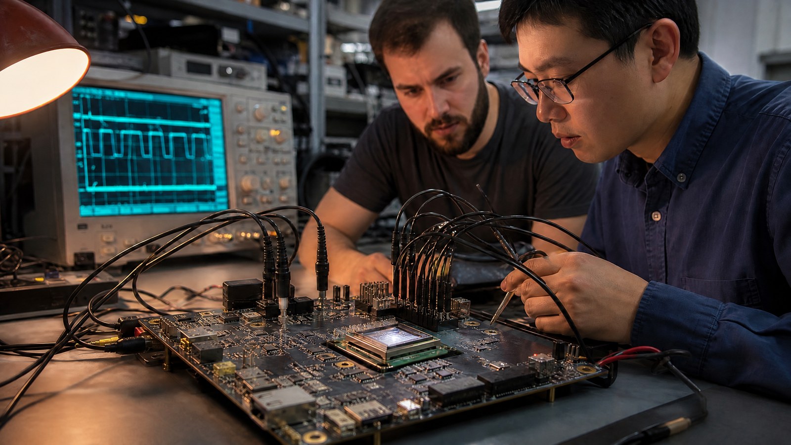
A processor need not be one uninterrupted piece of silicon. A chiplet approach divides functions among smaller dies and then reunites them in one package. That shifts difficult work rather than removing it: signals must cross die boundaries, power must arrive cleanly, heat must leave, and every die must be known-good before and after assembly. The useful question is therefore not whether a design uses chiplets, but whether its package-level system is coherent.
This article is part of the computer hardware technology guide library.
The boundary moves from die to package
A chiplet is a separately manufactured integrated-circuit die intended to work with other dies in a shared package. It can hold a compute block, input/output logic, cache, or another specialised function. This division lets a designer choose different manufacturing processes or reuse a validated block. The resulting product is a system-in-package: the package becomes an active engineering layer rather than merely a protective enclosure around a single processor.
That new boundary creates interfaces that a monolithic die keeps inside silicon. Clocks, data, control signals, power, and test access must cross it reliably. The UCIe Consortium describes its standard as a package-level die-to-die interconnect spanning physical-layer I/O, protocols, software considerations, and compliance testing. An open link can reduce interface ambiguity, but it does not make separate dies electrically or mechanically interchangeable by itself.
Packaging is an electrical decision
Advanced packaging places dies on or above a substrate that routes thousands of short connections. A two-dimensional arrangement positions dies beside one another; a 2.5D design commonly uses a high-density interposer between them and the package substrate; a three-dimensional arrangement stacks active dies. These labels describe geometry, not a universal performance ranking. Routing density, available area, signal integrity, power delivery, and assembly yield all change with the chosen construction.
Interconnect distance matters because fast electrical links consume energy and lose signal quality as their channels become harder to drive. Short, dense package routes can therefore be attractive for high-traffic connections. They also introduce tight pitch, alignment, and thermal constraints. IEEE’s heterogeneous-integration roadmap treats packaging, interconnect, test, materials, processes, and equipment as linked technical subjects. In practice, an interposer decision is also a decision about manufacturing flow, inspection, and how a completed package can be debugged.
A die-to-die link needs more than speed
A die-to-die interconnect is the communication path between chiplets. It includes physical signalling, link training, error handling, protocol rules, and sometimes management features. Designers care about bandwidth, latency, energy, and usable reach, but those measures are incomplete without interoperability and fault behaviour. UCIe explicitly covers a physical layer, protocols, a software model, and compliance testing, illustrating why a link specification is broader than the number of wires or the data rate.
Using a common interconnect can make a design easier to partition and can support a broader component ecosystem. The trade-off is that a standard interface may not capture every specialised optimisation a single organisation would make for a tightly controlled product. Custom links can target a particular topology, while open links aim to establish a repeatable contract. Either path still requires disciplined system validation, including reset, power-state, error, and performance behaviour across the actual assembled package.
Known-good die is necessary, not sufficient
Testing a chiplet before assembly is valuable because a package may contain several expensive parts. Yet a die that passes standalone tests can still fail in its final context. Package assembly can introduce mechanical stress, interconnect defects, altered power behaviour, or different thermal conditions. A credible test plan therefore follows the product lifecycle: wafer-level checks, assembly inspection, package-level electrical test, and diagnostics that remain usable after a system is deployed.
Design-for-test and design-for-debug are ways of reserving observability and control before hardware is built. The UCIe 2.0 overview highlights manageability, testing, telemetry, and debug across a multi-chiplet system-in-package lifecycle. This is not decorative infrastructure. When failures can originate in a die, a bond, a route, firmware initialisation, or a protocol interaction, isolating the cause without planned visibility becomes materially harder. Modularity raises the value of clear ownership and diagnostic boundaries.
Heat and power do not respect module boundaries
Chiplets may separate functions on a floorplan, but heat spreads through silicon, interfaces, and package materials. A hot compute die can affect neighbouring memory or input/output dies, while vertical stacking changes the path from an active layer to the cooler. Power is equally shared: the package and board must deliver current without excessive voltage variation as multiple dies change activity. A good partition is one whose electrical and thermal behaviour remains manageable under realistic concurrent work.
The design trade-off is not simply more integration versus less. Bringing functions together can shorten data paths, while concentrating active blocks can complicate cooling and power delivery. Spreading functions can ease one local hotspot but increase interface traffic and routing. Engineers model these interactions early and validate them later with package-aware measurements. Treating thermal and power design as late mechanical tasks risks discovering that an elegant logical partition cannot sustain its intended operating conditions.
How to read a chiplet claim
When evaluating a chiplet architecture, start with the workload boundary. Ask which functions exchange the most data, which require distinct manufacturing technologies, and which must remain coherent. Then identify the package geometry and the link contract. A useful explanation states what is standardised, what remains proprietary, and what assumptions are made about topology. It should not imply that a chiplet label alone guarantees lower cost, higher performance, or multi-vendor compatibility.
Next, look for lifecycle evidence: pre-assembly test, package test, error reporting, power sequencing, and thermal limits. These details reveal whether modularity has been engineered as a system property. The enduring lesson is straightforward. Chiplets make processor composition more flexible, but the package is where that composition becomes physical. Interconnect discipline, manufacturability, and serviceable observability decide whether the flexibility translates into a dependable product.
Source notes
Reporting record
techduopulse stores source destinations privately. Public notes remain non-clickable so every visitor journey stays on this website.
UCIe package-level interconnect specifications
Primary source · Package-level interconnect, compliance, manageability, and 3D packagingIEEE heterogeneous-integration roadmap
Primary source · Packaging, interconnect, test, materials, processes, and equipment contextInitial reviewed edition grounded in standards and institutional technical documentation.