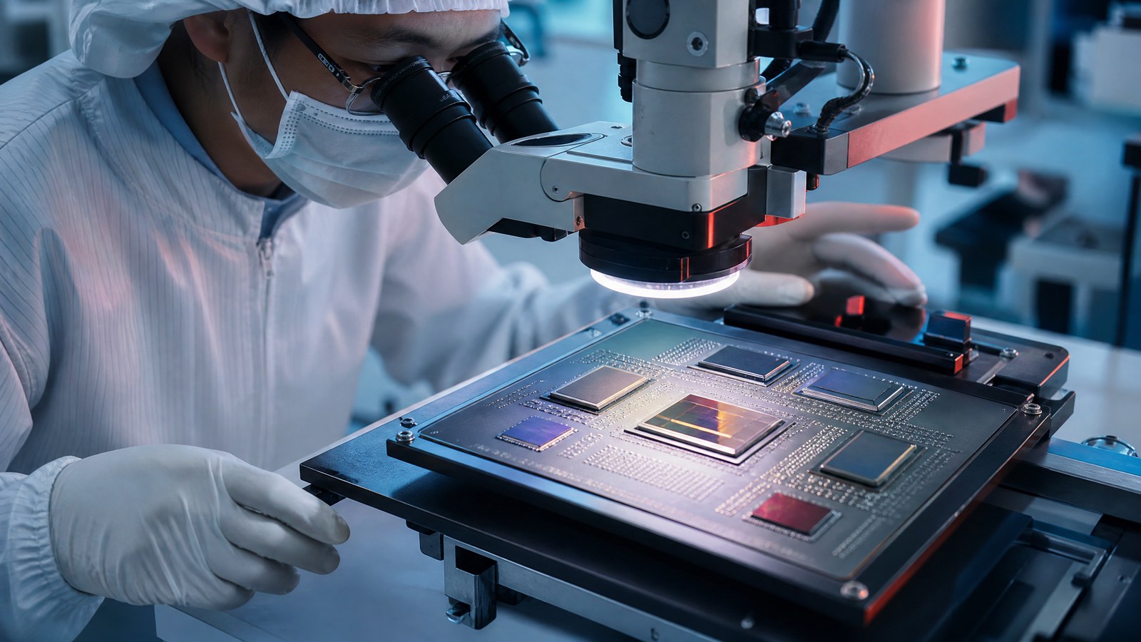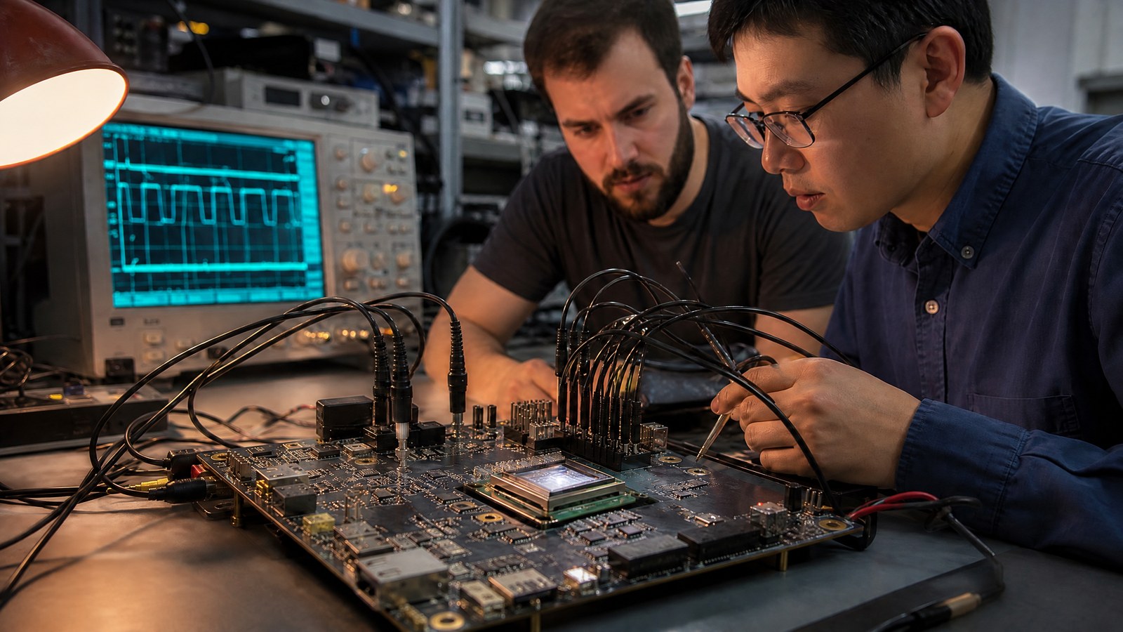
A wafer can hold many copies of a chip design, yet not every copy will meet its electrical and functional specification. The proportion that does is yield. Yield is a manufacturing and design outcome, not a single machine setting. It reflects defects, process variation, design sensitivity, test coverage, and the ability to find causes quickly. That is why apparently small changes in defect control can have outsized consequences: a defect mechanism repeated across a wafer can turn a promising process into a constrained source of usable die.
This article is part of the computer hardware technology guide library.
Yield is a pass rate with context
Semiconductor yield is commonly expressed as the proportion of fabricated die that pass the required tests. A wafer-level number is useful, but it needs context: what test limit was used, which failures were screened, and whether the product includes redundancy or repair features. Yield should not be confused with the number of die physically printed on a wafer. It is the count of acceptable devices relative to the opportunity, after a defined manufacturing and test process has been applied.
Different kinds of yield can be discussed separately, including wafer yield, die yield, parametric yield, and final test yield. Parametric yield concerns devices that function but miss a required electrical margin, such as timing or leakage limits. A device may also fail because a physical defect interrupts or shorts a feature. Separating these categories helps engineers avoid treating all failures as the same problem. The corrective action for contamination may differ from the action for a design-process interaction.
A defect becomes costly when it is critical
A defect is an unintended imperfection in material, pattern, or structure. Not every observed imperfection causes a product failure. A critical, sometimes called killer, defect is one that affects a circuit feature enough to prevent the device from meeting specification. Whether a defect is critical depends on its position, size, the design’s tolerance, and the process architecture. This is why raw defect counts alone do not explain yield; engineers need a defensible connection between observed signatures and failing die.
NIST’s work on optical volumetric inspection describes a practical obstacle: optical scattering from a yield-impacting defect can be obscured by scattering from other variations, called wafer noise. As features shrink and patterns become more complex, distinguishing a relevant signal from background variation is difficult. A false positive sends attention to a harmless feature; a missed defect allows a real yield mechanism to persist. Inspection value therefore depends on sensitivity, context, and the quality of subsequent review.
More area creates more opportunities for loss
All else equal, a larger die spans more process area and more circuit features, giving random defect mechanisms more opportunities to intersect something critical. The relationship is not a fixed rule that applies identically to every technology. Defects can cluster, designs have unequal sensitivity, and redundancy can change outcomes. Still, this basic geometry helps explain why yield analysis is inseparable from product architecture. A design decision that adds area can change both capability and exposure to manufacturing variation.
The International Technology Roadmap for Semiconductors grouped yield work around models and defect budgets, detection and characterisation, and wafer-environment contamination control. A defect budget translates a product yield target into control objectives for process steps. It is a planning tool, not a guarantee. As designs and processes change, historical relationships can fail to transfer cleanly. Teams continually revise their models using inspection, electrical test, process data, and physical analysis rather than relying on a single historical average.
Measurement determines how quickly teams learn
Metrology is the science and practice of measurement. In semiconductor production it includes measurements that reveal dimensions, layer properties, alignment, defects, and electrical behaviour. NIST notes that increasingly complex, small, and multilayer devices make it harder to measure, monitor, predict, and assure manufacturing quality. If measurement tools cannot resolve a relevant change reliably, engineers cannot confidently connect it to a yield shift or know whether a corrective action worked.
A useful inspection flow narrows uncertainty in stages. Broad wafer inspection can identify locations or patterns worth review; higher-resolution analysis can classify a suspected mechanism; electrical test can show the functional consequence; and process history can suggest where to investigate. Each stage has limits in throughput, cost, and confidence. The goal is not to collect every possible image, but to build enough correlated evidence to distinguish a real yield limiter from measurement noise, incidental variation, or a one-off event.
Yield learning is a feedback system
Yield learning is the process of turning failure data into changes that improve the rate of acceptable output. It links design, process integration, equipment, facilities, inspection, test, and analysis. The roadmap specifically calls for intelligent analysis that correlates facility, design, process, test, and work-in-progress data to improve root-cause analysis. This systems view matters because a defect signature may originate in a material, tool condition, design pattern, handling step, or interaction between several of them.
Fast learning does not mean reacting to every fluctuation. It requires controls that distinguish normal process variation from a meaningful excursion, and experiments that can test a plausible cause. A correction may reduce one class of failure while affecting another process margin, so confirmation matters. The most reliable yield narratives describe the chain of evidence: what failed, how it was observed, how it was traced, what changed, and what result was verified. Correlation alone is an investigative lead, not a conclusion.
Economics follows usable output
Manufacturing cost is influenced by the resources consumed to make a wafer and by how many acceptable die emerge from it. If fewer die meet specification, more wafer processing may be needed to supply the same number of finished parts. That relationship is why yield can reshape product economics without any change to the nominal wafer price. It also explains why teams invest in defect reduction, measurement capability, and design-for-manufacturability: they affect the usable outcome rather than merely the activity count.
The responsible conclusion is not that every small defect-rate improvement has the same financial effect. The outcome depends on die area, failure distribution, test limits, repair options, demand, process maturity, and the cost of the intervention. What remains evergreen is the mechanism. Yield turns manufacturing variation into usable-device availability. Understanding criticality, measurement limits, and feedback loops is more informative than quoting an isolated yield percentage without the product and test context behind it.
Source notes
Reporting record
techduopulse stores source destinations privately. Public notes remain non-clickable so every visitor journey stays on this website.
NIST semiconductor metrology program
Primary source · Measurement challenges, production yields, quality, and costNIST wafer-defect inspection study
Context source · Defect signal, wafer noise, false positives, and overlooked defectsITRS yield-enhancement roadmap chapter
Primary source · Defect budgets, detection, characterisation, contamination control, and yield learningImage updated: embedded writing removed; article content and factual claims unchanged.