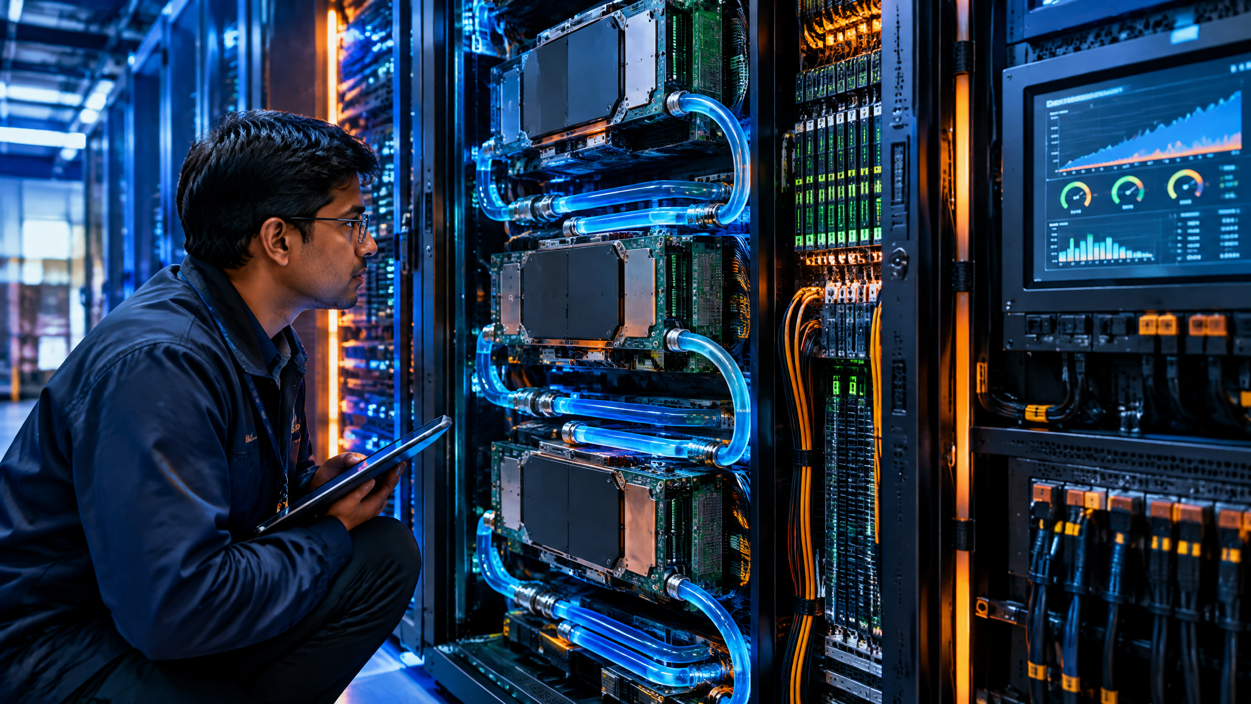
An AI chip is not simply a faster processor. It is part of a tightly connected system that must perform many matrix calculations, keep model data close to the compute units, move information quickly between components and stay within power and cooling limits. That is why conversations about AI chips increasingly include chiplets, high-bandwidth memory (HBM), advanced semiconductor packaging and networking—not only the processor itself. For a general reader, the useful mental model is this: an AI service needs compute to do the maths, memory to hold model data and working state, and interconnects to move data among those resources. The package around the silicon can determine how well those parts work together. This article explains the pieces and the trade-offs without treating a single product or benchmark number as the whole story. Key Takeaways
This article is part of the software engineering technologies guide library.
What is an AI chip?
An AI chip is a processor or accelerator designed to run machine-learning workloads efficiently. Neural networks repeatedly perform operations such as multiplying large arrays of numbers and adding the results. A general-purpose CPU can do that work, but it is built to handle a wide range of tasks, including branching, operating-system work and diverse application logic. An accelerator concentrates more hardware and data paths on the highly parallel calculations common in AI.
Google’s TPU documentation offers a clear example of the distinction. It describes TPUs as application-specific integrated circuits (ASICs) for machine learning, with matrix multiplication units formed from systolic arrays; data is staged through HBM for the computation. [1] A GPU takes a different design route: it remains broadly programmable while exposing many parallel compute units. In practice, an AI deployment can use CPUs, GPUs, dedicated ASICs, neural processing units (NPUs), memory and networks together.
### CPU, GPU, NPU and ASIC: the useful distinction
A CPU coordinates general software, prepares data and handles work that does not parallelise well. It remains essential even in many accelerator-heavy servers.
A GPU can execute many similar operations in parallel and has a mature software ecosystem for AI as well as graphics and technical computing.
An NPU or ASIC is usually more specialised. It may be built around a narrower set of numerical operations or power limits, such as on-device AI or a cloud service’s chosen model types.
An AI accelerator is the umbrella term. It can refer to a GPU, TPU, NPU, ASIC or another processor used primarily for AI workloads.
These are architecture categories, not automatic rankings. A specialised design can be efficient for a target workload yet less flexible when a model, framework or numerical format changes. A general-purpose GPU may be easier to use across changing workloads but may not be the best fit for every power, cost or latency constraint.
### Training and inference use the same ideas differently
Training adjusts a model’s parameters using very large sets of examples. Inference uses an already trained model to produce a classification, prediction, image, token or other output. Both can require significant compute and memory, but their operating constraints differ.
An inference service may need a low response time for each request, high total throughput for a batch of requests, or both. A small model running locally in a device has different constraints from a large service spread across data-centre servers. So “best inference chip” is not a meaningful conclusion without the model, precision, request pattern, latency limit, power boundary and software stated alongside it.
Why the package has become part of AI-chip performance
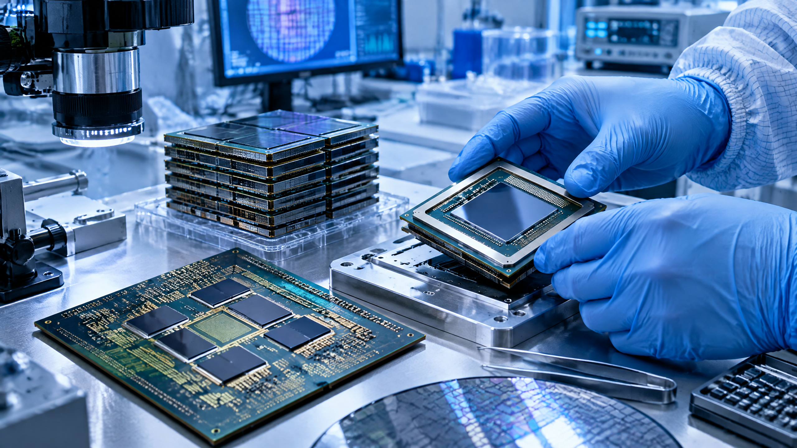
A silicon die is the piece of semiconductor made on a wafer. Packaging is the set of technologies that connect, protect, power, cool and test one or more dies so they operate as a system. It is not merely a protective shell.
Modern packaging may place compute dies, memory stacks and interconnect structures close together. Intel describes its foundry packaging portfolio in terms of 2D, 2.5D and 3D system-level integration and test. [2] TSMC’s CoWoS platform similarly describes a wafer-level integration approach with varying interposer sizes, HBM cube counts and package sizes for high-performance computing. [3]
The reason is straightforward: AI processors can become constrained by getting data to the arithmetic units. Compute engines cannot deliver their theoretical output when needed model weights or intermediate data arrive too slowly. Shorter and wider package-level paths can help, but they make electrical design, thermals, assembly and validation more complex.
### 2D, 2.5D and 3D—without the jargon overload
2D packaging places dies next to one another on a package substrate. It is the familiar starting point for many multi-chip designs.
2.5D packaging puts multiple dies beside one another on a high-density interconnect layer, often called an interposer or bridge. It is a common way to bring compute and HBM close together with many connections.
3D packaging stacks dies vertically, creating shorter paths in some designs. It can raise density, but heat removal, manufacturing yield and test strategy become particularly important.
Observed fact: Foundries and packaging suppliers describe 2D, 2.5D and 3D integration as distinct system-level packaging approaches. [2] [3]
Interpretation: As workloads become more sensitive to data movement, package engineering becomes a system design decision rather than a final assembly step. That does not mean every AI product needs the most complex package.
Chiplets: building one processor from several pieces
A chiplet is a functional piece of silicon designed to work with other dies in the same package. One chiplet might focus on AI compute, another on input/output, cache or a specialised function. The result can look like one processor to the system even though it contains several dies.
This approach can let designers use different manufacturing processes for different functions and avoid making every part of a large design on the same die. It can also create reusable design blocks. But a chiplet-based product is successful only if data can cross the die-to-die links reliably, quickly and with acceptable energy use.
UCIe (Universal Chiplet Interconnect Express) is an open specification for interconnects between chiplets within a package. Its stated initial focus includes physical die-to-die I/O and near-term CXL/PCIe protocol attachment. [4] This is important because a shared interface can make an ecosystem more feasible. It does not mean chiplets from any vendors can automatically be combined in any package; electrical, physical, thermal, validation, commercial and software requirements still apply.
NVIDIA’s Blackwell architecture is a current vendor example of why multi-die design matters: NVIDIA states that its Blackwell products use two reticle-limited dies linked at 10 TB/s to form a unified GPU. [5] The observation is about that architecture, not proof that two dies are inherently better than one. The better design depends on the workload and the total system.
### What chiplets change—and what they do not
Potential benefits include modular design, use of process technologies suited to different functions and a path around the practical difficulty of making one very large die. Potential costs include extra interfaces, more complex packaging, difficult fault isolation and additional power or latency whenever data crosses a boundary.
Chiplets do not remove the need for good software. Compilers, communication libraries, memory management and scheduling must make useful use of the hardware layout. A system with more compute dies can still perform poorly if its memory or communication path is the bottleneck.
HBM memory: why AI accelerators need wide data paths
High-bandwidth memory (HBM) is stacked DRAM designed to give a processor a very wide interface to memory in a compact package-level arrangement. It is memory, not compute: HBM holds model parameters, activations and other working data while the accelerator performs calculations.
The current HBM4 standard illustrates the direction of travel. JEDEC announced JESD270-4 on 16 April 2025 with transfer speeds up to 8 Gb/s across a 2,048-bit interface and total bandwidth up to 2 TB/s. The standard also defines 32 channels per stack, compared with 16 for HBM3. [6] Those are specification-level capabilities; actual system results depend on the controller, package, cooling, model and software.
### Bandwidth and capacity solve different problems
A useful distinction is:
Bandwidth is how much data can move in a given time. It matters when compute units are waiting for weights or other data.
Capacity is how much data can reside in memory at once. It matters when a model, its working state and a service’s active requests must fit without excessive transfers or splitting.
A system can have high bandwidth and still be capacity-limited. It can have ample capacity but deliver poor response time if access and communication are poorly arranged. For language models, the active context and key-value cache can add material memory demand during generation, so the right answer changes with prompt length, concurrency and serving design.
HBM also has trade-offs. The dense, high-speed connection it enables pushes more of the system’s value and complexity into advanced packaging. Memory availability, package yield, thermal behaviour and qualification can affect the finished accelerator. It is therefore misleading to describe HBM as a simple plug-in upgrade.
Inference hardware: performance is a system property
Inference is where a deployed model turns inputs into outputs. For a chatbot, that can mean producing tokens. For a vision system, it may mean classifying frames. For a factory or phone, it may mean making a local decision without sending data to a distant server.
An AI inference accelerator attempts to execute this work with suitable latency, throughput and energy use. It does so through more than arithmetic hardware. Memory capacity and bandwidth, interconnects, numerical precision, compiler support, batching, runtime scheduling and model optimisation all influence the outcome.
NVIDIA’s TensorRT-LLM documentation, for example, lists techniques including custom attention kernels, in-flight batching, paged key-value caching, quantisation, speculative decoding and parallelism for inference on NVIDIA GPUs. [7] The broad lesson is vendor-neutral: software and model choices can change the way a given hardware system behaves. The specific library is optimised for NVIDIA platforms and should not be used as an impartial cross-vendor comparison.
### The metrics that deserve to travel together
When assessing inference hardware, keep these questions together:
What model and quality target were used? A faster result at lower precision or lower quality is not automatically comparable to another result.
What is measured—latency, throughput or both? A system that processes many requests per second may not give the fastest response to one user.
What is included in the measurement? A chip-only figure may omit host CPU work, networking, memory, storage, cooling or power conversion.
What software stack was used? Drivers, kernels, compilers, libraries and serving settings can materially affect results.
Is it available, preview or research hardware? Availability changes the practical meaning of a result.
MLCommons’ MLPerf Inference: Datacenter suite measures how quickly systems process inputs and produce results using trained models. It defines scenarios with latency constraints, throughput metrics and compliance rules. It also classifies submissions by availability and distinguishes closed and open divisions. [8] That structure is a useful reminder: credible comparisons name the workload and conditions rather than relying on a bare operations-per-second number.
A practical way to connect chiplets, HBM and inference
These terms describe different layers of one system:
Compute engine: GPUs, TPUs or other accelerators run matrix and related operations.
Memory: HBM or other memory holds model data and working state.
Package: Advanced packaging brings compute, memory and dies together with appropriate electrical, power and thermal connections.
Chiplet interconnect: If the design has several dies, die-to-die links carry traffic inside the package.
System interconnect: Links between accelerators, CPUs and servers become important when work spans devices.
Software: Frameworks and serving runtimes decide how model work, memory and requests are scheduled.
The bottleneck can sit at any layer. More compute will not cure an undersized memory configuration. Faster memory cannot fully offset poor software scheduling. Adding accelerators across servers can introduce communication overhead. This is why “AI chip performance” is best treated as a property of a defined system running a defined workload.
India context: design, packaging and AI hardware are distinct questions
India’s current technology agenda makes this topic locally relevant, but the terms must be kept separate. As of 13 October 2026, India Mobile Congress’s published 2026 SRISHTI track includes “Semiconductors / AI Chipsets” alongside AI-native telecom and edge/cloud themes. [9] This is evidence that the topic is on the event agenda; it is not evidence of a specific product’s availability, market share or performance in India.
The India Semiconductor Mission says its aim is to build a semiconductor and display ecosystem for electronics manufacturing and design. On its site, Semicon 2.0 is described as covering chip design, machines and materials, fabs, strengthening ATMP/OSAT, R&D and talent development. [10] ATMP means assembly, testing, marking and packaging; OSAT is outsourced semiconductor assembly and test. These are important parts of turning fabricated dies into validated components and products.
A Government of India PIB backgrounder dated 7 February 2026 likewise describes ISM 2.0 and attention to assembly, testing and packaging skills. [11] These are policy and programme statements, some of which include future targets. They should not be read as a guarantee that any particular leading AI accelerator, HBM stack or advanced package is made, offered or supported locally.
The practical India question for readers and organisations is usually narrower: where will the workload run, what data and latency constraints apply, and what support, power, connectivity and software skills are required? A phone, camera or industrial device may prioritise power and local response. A cloud deployment may prioritise flexible capacity and operations. Neither choice is inherently more “AI-ready.”
Limits and trade-offs to keep in view
AI hardware discussions often focus on peak compute. That can hide the conditions that decide real utility.
Power and cooling: Dense compute and memory generate heat. A design that fits a benchmark may require infrastructure that a smaller site or device does not have.
Memory pressure: HBM helps feed compute, but capacity still limits model size, context, batching and concurrent requests.
Packaging complexity: More advanced integration can increase density and bandwidth, while making yield, test, repair and thermal design harder.
Precision trade-offs: Reduced-precision formats and quantisation can lower memory use and speed computation, but quality must be evaluated for the intended task.
Interconnect overhead: Multi-chip and multi-server systems depend on fast communication. Data movement can limit scaling.
Software portability: A model that runs well on one accelerator and runtime may need conversion, new kernels or revalidation elsewhere.
Benchmark interpretation: Benchmark results are useful only when workload, model quality, configuration, system boundary and availability are comparable. [8]
The right conclusion is not that one architecture always wins. It is that a hardware decision should begin with the application’s measured needs and then test the complete system against them.
Frequently asked questions
### Are AI chips just GPUs?
No. GPUs are important AI accelerators, but AI workloads also run on CPUs, TPUs, NPUs and specialised ASICs. The useful choice depends on the workload, software, latency, energy and deployment environment.
### What is a chiplet in an AI chip?
A chiplet is one functional silicon die in a multi-die package. AI designs can use several chiplets connected inside the package. UCIe is one open specification intended for this kind of die-to-die interconnect. [4]
### Is HBM the same as RAM?
HBM is a type of DRAM, so it is memory, but it is designed and packaged differently from ordinary system memory. Its wide interface and close placement to an accelerator target high data bandwidth for demanding workloads. [6]
### Why does semiconductor packaging matter for AI?
Packaging determines how compute dies, memory and other components connect, receive power, shed heat and are tested. Advanced 2.5D or 3D approaches can support dense integration, but they also add engineering and manufacturing complexity. [2] [3]
### Is an AI inference accelerator only for chatbots?
No. Inference means using a trained model to create an output. That includes language generation, image recognition, recommendation, speech processing, anomaly detection and many other tasks.
### Does higher TOPS mean a faster AI system?
Not by itself. A headline compute number does not show memory capacity, memory bandwidth, latency, model quality, software efficiency, host work or power use. Compare measurements made on the same model and scenario instead.
### Are chiplets always cheaper or better than one large die?
No. Chiplets can improve design flexibility and enable different functions to use different die technologies. They also require high-quality interconnects, packaging, testing and software support. The trade-off depends on the product.
### Does semiconductor packaging in India mean that advanced AI chips are available locally?
No. Packaging initiatives, ATMP/OSAT capacity and policy programmes are meaningful ecosystem developments, but they do not by themselves establish the availability, origin or support status of a particular AI chip. Check a supplier’s current documentation for any product-specific claim.
The bottom line
AI chips are best understood as complete data-moving systems. Compute engines do the mathematics; HBM and other memory hold the data; chiplets and interconnects connect specialised pieces; advanced packaging makes the physical system possible; and software determines how effectively it is used.
That perspective cuts through simple “fastest chip” claims. For training or inference, ask what model is being run, what quality and latency it needs, where data lives, how the system is cooled and powered, and whether the software stack is proven for the workload. The answer will be more useful than a single peak-performance number.
Suggested same-site internal links (private editorial recommendations)
| Suggested anchor text | Recommended path | Why it helps the reader |
|---|---|---|
| chiplet design and package interconnects | /article/chiplet-design-packaging-interconnects-explained | Deepens the explanation of die-to-die communication and multi-die design. |
| HBM, CXL and the memory hierarchy | /article/memory-hierarchy-hbm-cxl-system-performance | Explains how bandwidth, capacity and memory tiers shape system performance. |
| semiconductor yield and manufacturing economics | /article/semiconductor-yield-defects-manufacturing-economics | Adds context for why large dies and complex packages involve trade-offs. |
| how smartphone processors work | /article/smartphone-processor-explained | Gives a consumer-device bridge for readers thinking about NPUs and on-device AI. |
| processor power delivery and cooling | /article/power-delivery-modern-processors-vrm-cooling | Provides practical context for power and thermal constraints in dense AI hardware. |
Frequently asked questions about AI Chips Explained: Chiplets, HBM, Packaging and Inference Hardware
These answers summarise the scope of this explainer. Availability, standards and implementation details can change, so check current official guidance before acting.
What is AI Chips Explained: Chiplets, HBM, Packaging and Inference Hardware?
AI Chips Explained: Chiplets, HBM, Packaging and Inference Hardware explains the main ideas, practical uses and limitations in plain English.
Why does this technology matter?
Its value depends on the problem, implementation, evidence, cost, security and the people responsible for using it.
What should readers verify?
Verify current availability, compatibility, security, privacy and regulatory details with the relevant official source.
Is this article professional or legal advice?
No. It is general technology information and does not replace professional, legal, regulatory or security advice.
Source notes
Reporting record
techduopulse stores source destinations privately. Public notes remain non-clickable so every visitor journey stays on this website.
India Mobile Congress 2026 official programme
Primary source · Research source 9Google Cloud TPU architecture documentation
Primary source · Research source 1Intel Foundry Advanced Packaging & Test
Primary source · Research source 2TSMC CoWoS advanced packaging platform
Primary source · Research source 3UCIe Consortium — About UCIe
Primary source · Research source 4NVIDIA Blackwell Architecture
Primary source · Research source 5JEDEC announces JESD270-4 HBM4 standard
Primary source · Research source 6NVIDIA TensorRT-LLM
Primary source · Research source 7MLPerf Inference: Datacenter
Primary source · Research source 8India Semiconductor Mission official site
Primary source · Research source 10PIB backgrounder: India Semiconductor Mission 2.0, 7 February 2026
Primary source · Research source 11New India-focused explainer covering AI chips explained, practical context, limitations and verified sources.