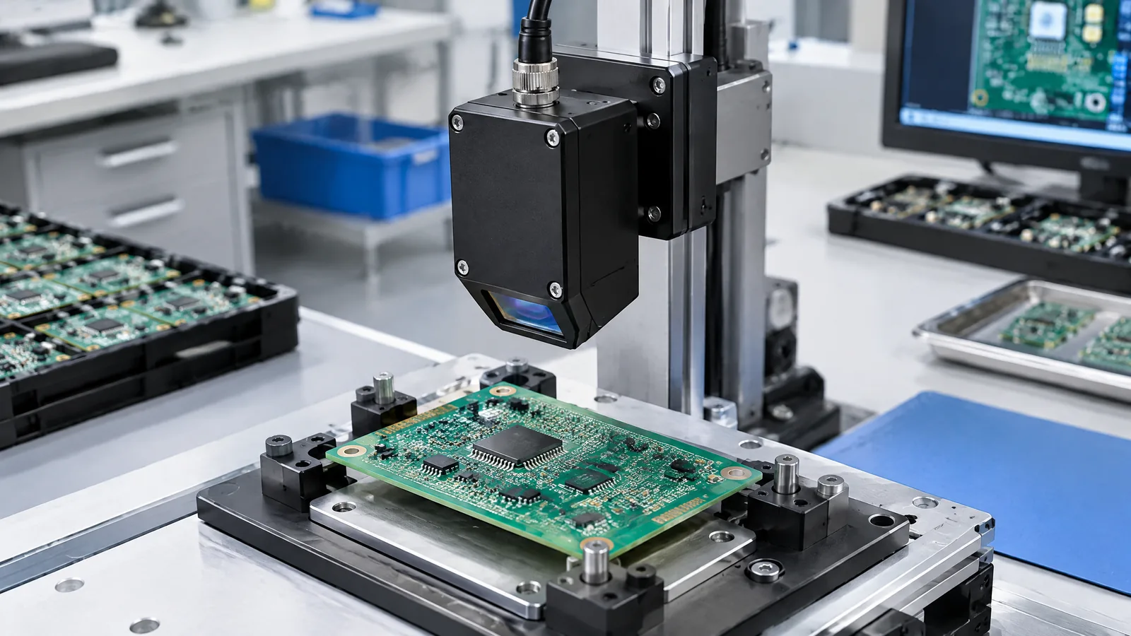
A PCB can look correctly placed while a connector, chip or soldered part is slightly too high for the next assembly step. A laser displacement sensor measures distance from a reference without touching the board, making it useful for checking component height, step height, thickness, warpage and position when the optical setup matches the material and range.
This article is part of the computer hardware technology guide library.
What a laser displacement sensor measures on a PCB
A laser displacement sensor is a measurement instrument, not a simple presence switch. It projects light at a target and converts the returned optical signal into displacement from the sensor's reference position. That value can be used to calculate height, thickness, width, position or a surface profile.
For electronics inspection, the target might be the top of an assembled component, a connector housing, a soldered joint, a board edge or the board surface itself. One point measurement can answer a local height question. A laser profiler or a moving stage can collect many points when the requirement is a line or 3D view of warpage. The profiler, motion stage and controller are external instruments or integration choices; they are not automatically part of the physical sensor head.
The practical question is therefore not only whether the sensor can see the board. It is whether the measured surface, reference plane, working range and sampling speed together represent the defect or placement tolerance that matters.
- Component height or step height relative to the PCB or a defined fixture reference.
- Board or substrate warpage by scanning several points and comparing their displacement values.
- Thickness, when the reference and optical arrangement are controlled; two opposing heads may be used for a moving or unsupported part.
- Position or alignment by comparing measured edges, features or heights with a known datum.
How laser triangulation turns light into distance
In a common laser triangulation arrangement, the emitter projects a spot and a receiving lens views the reflected spot from an offset angle. A CMOS or similar receiver sees the spot at a different position when the target moves nearer or farther away. The sensor processes that position into a displacement value.
Other optical methods use different information. Time-of-flight sensors calculate distance from the light's return time. Confocal displacement sensors determine which wavelength or focal condition corresponds to the target surface. These methods should not be treated as interchangeable labels: the target material, speed, geometry and required resolution influence which method is suitable.
For a PCB line, triangulation can suit fast, non-contact checks of component height or board position. A confocal head may be worth considering where transparent, glossy, dark or sharply shaped surfaces make ordinary triangulation difficult. The controller, output interface and inspection software remain system-level components that must be selected for the production workflow.
A useful inspection setup for PCB height and placement
Start with a stable datum. The sensor reports distance to the surface it sees, so a warped fixture or an inconsistent support can appear as a product error. Mount the head firmly, keep the optical path clear and place the target inside the specified measurement range rather than at an assumed distance.
For a single component-height check, the sensor can face the component top and compare the result with a board or fixture reference measured in the same coordinate system. For board warpage, move the board or sensor through a planned grid and retain the measured points. A conveyor, translation stage, encoder, PLC or data-acquisition system may be needed to synchronise position and readings; those are external integration elements, not the physical sensing principle.
Thickness needs extra care. One head can measure a part against a reference surface, but reference flatness, vibration and part warpage can enter the result. Two opposing heads can measure both surfaces of a moving part when their beams are aligned and their readings are synchronised. That dual-head arrangement is optional and application-specific, so a single sensor package should not be assumed to provide it.
Use the smallest useful measurement span rather than choosing a long-range head by default. In a given sensor family, a shorter span can provide more detector information per unit distance. Check the datasheet's stated resolution, linearity, repeatability, sampling rate and calibration conditions separately; resolution is not the same as accuracy across the full range.
- Define the reference plane and the feature to be measured before selecting the head.
- Check the sensor's working range, spot size, field of view and access around tall components.
- Rigidly fixture the head and board, and reduce vibration that could become measurement noise.
- Match the sampling period and board speed to the smallest feature or height change you need to detect.
- Decide how the controller will record a value, profile or pass/fail decision; the sensor alone does not define the inspection logic.
Surface, angle and environment limits
PCB assemblies are optically mixed. Solder, silkscreen, bare laminate, black packages and shiny metal can return different amounts of light. A dark or glossy area may produce a weaker or less stable triangulation signal, while a transparent or highly reflective surface may require a different optical method or a carefully tested angle. Do not transfer a catalogue performance value from a matte reference target to every board finish.
Keep the beam close to perpendicular to the intended surface when geometry allows. Tilt can create cosine error or change the reflected path, especially on reflective features. Edges, deep gaps and narrow spaces can also block either the emitted beam or the receiver's view. A different head orientation or a multi-point/profile arrangement may be needed, but it should be validated on the actual component layout.
Temperature, dust, smoke, a dirty protective window and fixture expansion can shift readings. Warm-up and environmental limits belong to the selected model's documentation. If a reading is unexpectedly unstable, inspect the reference surface, mounting, target finish and optical path before changing the pass/fail threshold.
What to verify before choosing a sensor
Ask the supplier or integrator to demonstrate the proposed head on representative boards, including the darkest, brightest, most reflective and most transparent surfaces in the inspection. A clean laboratory target cannot establish production performance on its own.
Confirm whether you need a single point, a laser line or a scanned 3D profile. Then compare the required height range and smallest feature with the sensor's range, spot size, resolution, linearity and sampling behaviour. If the board moves, include speed and synchronisation in the calculation rather than checking only the headline resolution.
Finally, define the safety and compliance review for the selected laser class and enclosure with the responsible equipment team. This article explains measurement selection, not a substitute for the manufacturer's laser-safety instructions, machine guarding review or site procedures.
- Target materials and finishes, including solder, package moulding, laminate and metal surfaces.
- Reference plane quality, fixture rigidity, board motion and access around components.
- Required range, resolution, linearity, repeatability, sampling rate and output interface.
- Whether one head, opposing heads, a line profiler, motion hardware or external lighting is required.
- Model-specific laser classification, operating limits and supplier validation on production-like samples.
Key takeaways
A laser displacement sensor measures distance from a reference, so it can inspect PCB height, step height, position, thickness or warpage rather than merely detect presence.
Triangulation is often suited to fast non-contact checks, but confocal or another optical method may be a better fit for difficult transparent, glossy or strongly varying surfaces.
Fixture flatness, alignment, surface reflectivity, vibration, sampling and working range can matter as much as the sensor's headline specification.
Treat controllers, stages, encoders, opposing heads and inspection software as optional system components that must be matched to the application.
Laser displacement sensor FAQs
Is a laser displacement sensor the same as a proximity sensor?
No. A proximity sensor commonly reports whether an object is present within a detection condition. A laser displacement sensor reports a measured distance or change from a reference, which can then be used for height, thickness, position or profile inspection.
Can one laser displacement sensor measure PCB warpage?
It can measure points along a board when the board or sensor moves through a planned path. A single fixed point only describes the surface at that location. A line profiler or 3D arrangement may be more appropriate when the complete surface shape is required.
Can it measure component height on a shiny or dark PCB assembly?
Possibly, but the result depends on the exact surface, angle, optical method and model. Shiny and dark surfaces can change the returned signal. Test representative parts and compare triangulation with confocal or another suitable method before treating the reading as production-ready.
How is PCB thickness measured without touching the board?
A controlled reference surface can support a one-head measurement, but its flatness and the board's warpage affect the result. For a moving or unsupported part, two opposing heads can measure both surfaces when aligned and synchronised. The arrangement is application-specific and may require external mechanics and a controller.
Does a higher resolution guarantee a more accurate inspection?
No. Resolution is the smallest change the sensor can reliably detect, while linearity describes error across the measurement range. Alignment, calibration conditions, target finish, fixture movement and sampling can limit the result even when the resolution number looks small.
About the image
AI-generated editorial illustration; not an actual product or mission photograph.
Source notes
Reporting record
techduopulse stores source destinations privately. Public notes remain non-clickable so every visitor journey stays on this website.
Source note: KEYENCE displacement-sensor and dimension-measurement guide
Primary source · Definition, PCB height/step, thickness, warpage, positioning, optical methods and electronics applicationsSource note: OMRON Displacement Sensor Technical Guide
Primary source · Triangulation spot-position principle, PSD/CMOS differences, sampling period, speed, resolution and linearitySource note: Acuity Laser laser-triangulation measurement guide
Primary source · Triangulation geometry, range, standoff, linearity versus resolution, alignment, environment, materials and dual-head thicknessSource note: KEYENCE laser displacement sensor technology and electronics applications page
Primary source · Triangulation and confocal comparison, component alignment, circuit-board handling and surface-related trade-offsInitial 15 October 2026 application explainer for the distinct inventory gap. Separates displacement measurement from presence detection; distinguishes the physical sensor from optional profilers, opposing heads, fixtures, motion hardware and controllers; and qualifies surface, alignment, range, sampling and model-specific laser-safety limits using four technical manufacturer sources.